Indium Nitride (InN): Heteroepitaxial Growth on Lattice Mismatched Substrates
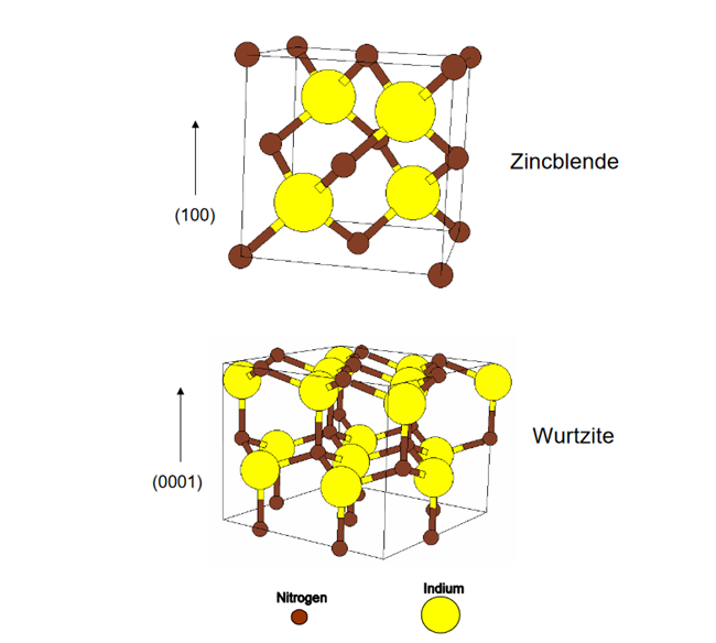
Nitride thin films occur commonly in two different phases. The lowest energy, and ther-modynamically stable crystal structure for Indium Nitride(InN), GaN and AlN is the wurtzite structure. The zincblende structure is closely related and of very similar energy. Consequently, by using a suitable template it is possible to grow the zincblende structure by non-equilibrium techniques such as MBE. This article will discuss the unit cell of InN for the wurtzite and zincblende structures[1].

Figure 1. The wurtzite and zincblende crystal structures[1].
As shows in above figure, the most common growth direction for wurtzite III-nitrides is the (0001) direction, also known as the c-axis. The c-axis is a polar direction which means that the crystal has an inherent electric field along this axis. The polarity arises from the lack of inversion symmetry in the wurtzite crystal which results in some charge separation along the c-axis. This can have consequences for surfaces and thin layers where the phenomena is most noticeable.
As no bulk nitride substrates are commonly available, growth of indium nitride has been performed on a number of different substrates and crystal orientations. The majority of this thesis considers growth on (0001) sapphire with the use of buffer layers. However, growth on quartz, (100) and (111) yttrium stabilised zirconia (YSZ) and (0001) GaN templates is also explored and discussed. Growing heteroepitaxially introduces a number of complications. Epitaxial growth requires a substrate to be chosen which has a surface template that matches the growth crystal symmetry. In the case of growing c-axis oriented wurtzite nitride thin films, this demands hexagonal symmetry on the substrate surface.
The next major consideration is lattice mismatch of indium nitride crystal. Any mismatch between the lattice constants of the substrate and the film can lead to misfit dislocations. Dislocations can propagate through III-V thin films and significantly degrade the optical properties of the layer. Many techniques such as nitriding and inserting buffer layers have been developed to accommodate misfit strain but it remains one of the foremost problems. A close match between thermal expansion coefficients is also important. As a film cools down from the growth temperature both the substrate and film will contract. If there is a significant difference in the thermal expansion coefficients then this may cause the film to crack. Cracks can result in regions of the indium nitridefilm becoming electrically isolated from each other, rendering the film useless for devices.
Reference
[1] Phillip A. Anderson. Indium Nitride: An Investigation of Growth, Electronic Structure and Doping. PhD thesis, University of Canterbury, May 2006.


