Crystal and Surface Electronic Structure of Holmium Silicide
The surface electronic structure of two- and three-dimensional holmium silicide grown on Si(111) has been studied with the techniques of metastable de-excitation spectroscopy (MDS) and ultraviolet photoemission spectroscopy. Electronic structure differences between the two cases are examined, and the extreme sensitivity of MDS to the surface density of states (DOS) allows a direct comparison between deconvolved spectra and ab initio density-functional theory calculations.
This comparison shows a good agreement between the DOS calculated for the Si(111)-1×1-Ho structure and MDS data obtained from an almost-complete layer of two dimensional holmium silicide. The dominant role of the topmost silicon bilayer in determining the surface electronic properties is revealed.
The atomic and electronic structures of both 2D and 3D RE silicides on Si(111) have been studied with a number of techniques including medium-energy ion scattering (MEIS), low-energy electron diffraction (LEED), scanning tunneling microscopy (STM), Auger and photoelectron diffraction, and surface x-ray diffraction(SXRD).

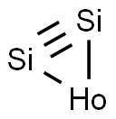
This research has revealed strong similarities in the structure formed when different trivalent RE metals (e.g., Dy, Ho, and Er) are deposited on Si(111) and the structural models deducted are shown in Figure 1[1]. For a 2D holmium silicide, Ho atoms are positioned in the T4 sites of the substrate Si forming a single layer, above which sits a buckled Si bilayer of opposite buckling direction to the bulk (type B buckling, as opposed to type A buckling in which atomic positions mirror those of the bulk-terminated surface). The reverse buckling occurs as the configuration of Si atoms results in the maximum number of nearest neighbors for each RE atom therefore stabilizing the structure. Among the three valence electrons of the trivalent REs available for bonding, two directly bond to the upward- and downward-pointing dangling bonds (DBs) of the substrate and surface bilayer Si atoms, respectively, forming a saturated closed-shell structure[2].
References
[1] Crystal structure of holmium trisilicide, HoSi3. Z. Kristallogr. NCS 226 (2011) 297-298. DOI: 10.1524/ncrs.2011.0131
[2] Surface electronic structure of two- and three-dimensional holmium silicide on Si(111). PHYSICAL REVIEW B 79, 245406, 2009.